|


 |  |

| Aeronautica | Comunicatii | Drept | Informatica | Nutritie | Sociologie |
| Tehnica mecanica |
Comunicatii
|
|
Qdidactic » stiinta & tehnica » comunicatii Modul PKE-Receptor/Decodor |
Modul PKE-Receptor/Decodor
Modul PKE-Receptor/Decodor
1.Introducere
Modul consta intr-un receptor UHF, un microcontroler, o sursa de alimentare, LED-uri, indicatoare si o interfata.
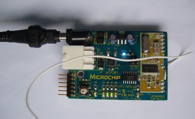
Anexa8:Poza modulului receptor/decoder
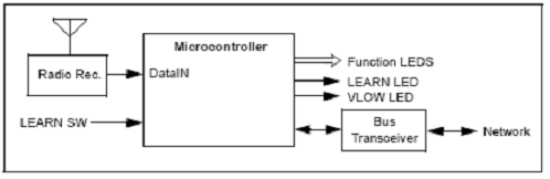
Figura1
2. Hardware-ul
2.a. Receptorul UHF
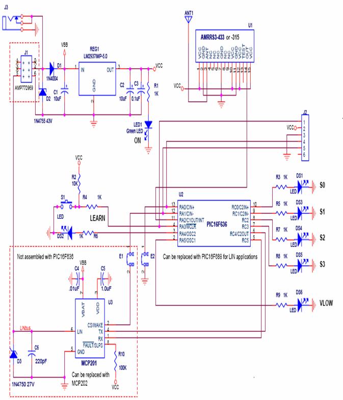
Intrarea RF este un modul hibrid compact AM super-regenerativ, ce se utilizeaza la reactia semnalului necodat de la emitatorul AM. Acest modul este foarte stabil in frecventa intr-o gama larga de temperaturi. O bobina cablata elimina nevoia unor componente ajustabile. O iesire compatibila TTL/CMOS-accepta date de transfer de pana la 2MHz. Aceasta intrare a modulului receptor este conectata la portul A la microcontroler.
2.b.Microcontrolerul
Acesta poate fi oricare PICmicro cu 14 biti dar de obicei se utilizeaza un PIC16F636 sau PIC16F688. Primul are intergrat encoderul KEELOQ in timp ce al doilea are portul USART (EAUSART) ce suporta protocolul interfetei LIN si al J2602
|
PORT Pin |
Functii |
Note |
|
Intrari |
||
|
RA0 |
Jumper E2 to GND, available to user |
ICSP Data |
|
RA2 |
Intrarea Data RF |
|
|
RA3 |
Invata apasarea butonului de intrare |
ICSP MCLR |
|
Iesiri |
||
|
RA4 |
Invata modul de activare LED |
|
|
RA5 |
VLOW LED |
|
|
RC0 |
Functia S0 a LED-ului |
|
|
RC1 |
Functia S1 a LED-ului |
|
|
RC2 |
Functia S2 a LED-ului |
|
|
RC3 |
Functia S3 a LED-ului |
|
|
Reteaua de emisie-receptie |
||
|
RA1 |
Selectarea iesirii din chip |
ICSP Clock |
|
RC4 |
Iesire TX |
|
|
RC5 |
Intrare RX |
|
Interfetele
Un
transceiver LIN-MCP201 se utilizeaza pentru a realize fizic bus-ul slave
ce trebuie conectat la o interfata LIN compatibila. O dioda
Zenner protejeaza bus-ul de tensiuni tranzitorii.Un rezistor "pull-up" la pinul ![]() /SLPS - asigura ca
dispozitivul se reseteaza la o
anumita panta de tensiune.
/SLPS - asigura ca
dispozitivul se reseteaza la o
anumita panta de tensiune.
2.d.Modulul de alimentare
Tensiunea de alimentare poate
ajunge fie printr-un conector jack (J3), fie prin J1 (AMP770969) si trebuie sa fie cuprins in plaja
8÷18![]()
Conectori
Sistemul de conector J1
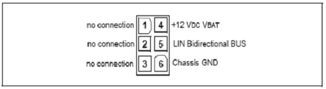
Figura2
Programarea conectorului J2

Figura3
Puterea conectorului J3
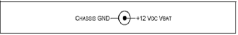
Figura4
Anexa9: Schema circuitului receptor/decoder
2.d.Familia PICmicro-Mid-range cu decoder de cod
"saritor"(happing code)
Este descris decloderul de cod "saritor" KEELOQ, implementat in capsula microcontrolerului PIC16CE624(figura5).
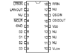
Figura5
Softul a fost realizat ca un grup de module independente. Pentru claritate fiecare modul acopera o singura functie.
Caracteristici cheie
Setul de module ce urmeaza a fi prezentat implementeaza urmatoarele caracteristici:
mod de invatare normala;
poate memora codurile a 16 emitatoare utilizand memoria interna EEPROM;
poate lucra in intreruperi furnizate de semnale PWM;
este compatibil cu toate decodoarele KLEEQ cu formatul de transmisie PWM selectat operand in "slow-mode" (TE=400µs);
este compatibil cu decodorul HCS512;
poseda un oscilator RC cu autocalibrare in timpul receptiei.
|
Nume Pin |
Numar Pin |
Intrare/Iesire |
Functii |
|
RF IN |
18 |
1 |
Demoduleaza semnalul PWM din receptorul RF |
|
LEARN INIT |
1 |
1 |
Intrarea in modul de invatare |
|
LEARN LED |
2 |
0 |
Afisarea in iesire a statusului procesului de invatare |
|
S0, S1, S2, S3 |
6, 7, 8, 9 |
0 |
Functiile de iesire corespunzatoare pinilor de intrare a encoderului |
|
VLOW |
10 |
0 |
Transmiterea prin encoder a starii bateriei |
|
|
14 |
PWR |
Sursa de alimentare de 5V |
|
|
5 |
GND |
Masa comuna |
Reprezentarea modulelor
Codul prezentat este compus din urmatoarele module de baza:
RXI.INC - receptor in intrerupere;
KEYGEN.INC - generarea de rutine KEELOQ in modul normal;
FASTDEC.INC - rutina KEELOQ de decriptare;
MEM-62X.INC - drivere pentru memoriile EEPROM ale microcontrolerului;
TABLE.INC - memoria tabelului;
MID.ASM - initializare si bucla principala
Prezentare modulelor
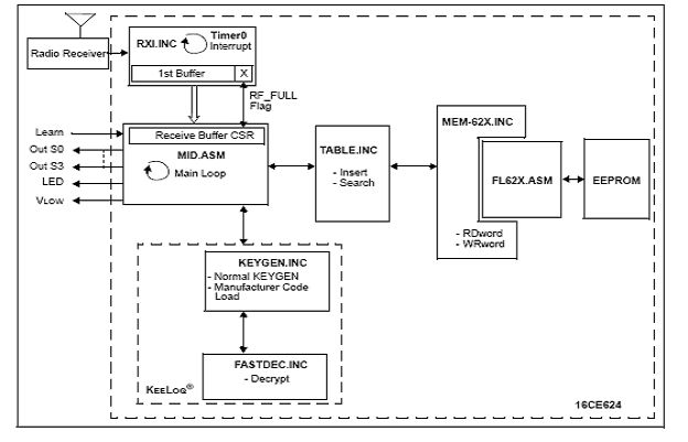
Figzra6
2.e.Modulul receptor
Intreaga rutina de receptie a fost implementata intr-un mod in care poate opera cu o baza de timp fixa (ce poate fi utilizata pentru crearea de timere virtuale). Modul de lucru pentru aceasta rutina (ISR) este complet transparent pentru programul principal fiind similar portului UART. De fapt rutina de intrerupere consuma aproximativ 30% din puterea de calcul a microcontrolerului.
Dupa ce un cuvant de cod de 66 biti transmisi a fost receptionat si stocat intr-un buffer de 9 biti, se seteaza un simplu flag (RF-FULL) si receptorul intra in modul " idle".
Este responsabilitatea programului principal sa utilizeze datele stocate in buffer si sa reseteze bitul flag pentru a valida o noua receptie.
Pentru a obtine o compatibitate maxima cu toate encoderele KEELOQ, cu sau fara posibilitatea de acord fin al oscilatorului, receptorul se recalibreaza periodic prin schimbarea periaodei de timp in concordanta cu lungimea pauzei caracteristice de sincronizare (TH=10XTE). Acest fapt ii permite decoderului sa functioneze cu un semnal de clock simplu (oscilatorul RC).
Forma codata a cuvantului transmis
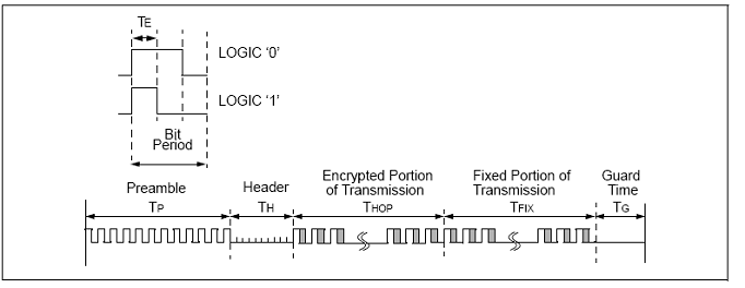
Figura7
Organizarea cuvantului codat
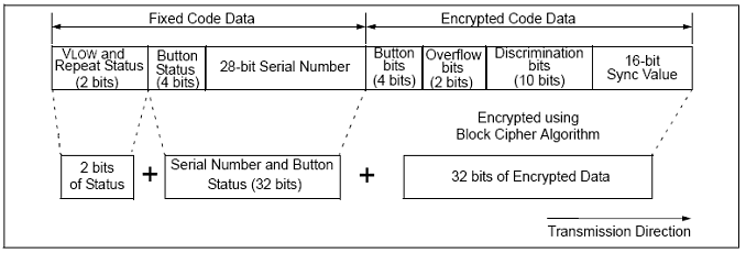
Figura8
Singurul periferic utilizat de rutina ISR este Timer si intreruperea de Overflow a acestuia disponibile pe orice microcontroler PICmicro din gama MID-RANGE.
Timer-ul este reancarcat la orice Overflow creand astfel timer-ul virtual pe 16 biti, numit XTMRH/XTMRL.
Rutina de receptie poate modifica perioada bazei de timp, in timpul receptiei celor 6biti ai transmisiei (crescand-o sau micsorand-o) pentru a se sincroniza si a compensa diferentele de clock dintre codor si decodor (encoder si decoder).
Modul de decriptare rapida
Acest modul contine implementarea algoritmului de decriptare KEELOQ ce a fost optimizat pentru viteza unui PICmicro din familia Mid-rage. Acesta permite timpi mici de raspuns chiar la viteze de 4MHz.
Functia de decriptare este utilizata in toate schemele de invatare si reprezinta un bloc fundamental al decodoarelor KEELOQ.
Modulul generator de cod (key generator)
Rutina de decriptare KEELOQ a modulului de decriptare rapida este utilizata pentru a genera o "cheie" la fiecare cuvant de cod receptionat.
Avantajul este o inregistrare a transmisiei mai mica, pe 8 biti, in loc de 16 biti. Acest lucru se traduce prin dublarea numarului de transmitatoare ce pot fi invatate utilizand memoria EEPROM de 128biti a microcontrolerului PIC16CE624. Aceasta reducere a spatiului ocupat in memorie prezinta insa dezavantajul unei puteri de calcul sporite pentru procesarea fiecarui cuvant de cod.
Cand un cuvant nu este receptionat este aplicat algoritmul "key generation" in mod "Normal Learn" rezultand o cheie de decriptare plasata in aria DKEY[0.7].
In timpul unei transmisii continue, cand utilizatorul tine apasat butonul transmitatorului, algoritmul key generation" nu este repetat.
Modulul Table
Unul din task-urile decodorului este acela de a mentine o baza de date ce contine toate codurile unice (IDs-serial numbers) ale transmitatoarelor invatate.
In cele mai multe cazuri baza de date poate fi un simplu tabel ce asociaza acele coduri memorate cu numaratoarele de sincronizare (ce stau la baza tehnologiei "cod saritor" happing
Fiecarui emitator invatat ii este atasata o inregistrare pe 8 biti ce contine toate informatiile relevante.
Inregistrarea transmisiilor
|
Offset |
Data |
Descriere |
|
+0 |
XF |
Function code 4 bits) and upper 4 Serial Number bits [24..28] |
|
+1 |
IDLo |
Serial Number bits 0..7] |
|
+2 |
IDHi |
Serial Number bits 8..15] |
|
+3 |
IDMi |
Serial Number bits 16. 23] |
|
+4 |
SYNCH |
Sync Counter 8 MSb |
|
+5 |
SYNCL |
Sync Counter 81 Sb |
|
+6 |
SYNCH2 |
Second copy of SyncH |
|
+7 |
SYNCL2 |
Second copy of SyncL |
Valoarea numaratorului de sincronizare pe 16 biti este memorata de doua ori, deoarece este cea mai importanta informatie. Aceasta este imbunatatita la fiecare apasare de buton a telecomenzii.
La citirea sincronizata a celor doua valori memorate, decoderul verifica daca cele doua valori sunt identice.
Varianta prezentata limiteaza la 16 numarul emitatoarelor ce pot fi memorate, aceasta datorita memoriei interne a microcontrolerului PIC16CE624.
Prin metoda simpla a listei liniare numarul poate ajunge la cateva zeci de coduri.Datorita simplitatii timpul de recunoastere a unui emitator creste liniar cu lungimea tabelului.
Este posibila atingerea unor tabele cu mii de coduri memorate prin inlocuirea modulului cu un tabel cu o structurare a datelor mai sofisticata, cum ar fi "Hash Table" sau cu un modul cu algoritmul de indexare.
Din nou datorita simplitatii solutiei curente nu este posibila stergerea selectiva a codului unui emitator memorat, ci a intregului tabel (Bulk Erase).
Acest lucru se intampla cand utilizatorul tine apasat butonul de "invatare" aproximativ
10 secunde. LED-ul se va stinge si la eliberarea butonului se va aprinde o data pentru a valida comanda de stergere.
Modulul MEM-62X
Acest modul este constituit in jurul unui set de rutine deja existent, special concepute pentru memoriile EEPROM a microcontrolerului PIC16CE62X.
Modulul permite accesul la memorie cu ajutorul a doua rutine Rdword si Wrword care cites, respectiv scriu valoarea codului pe 16 biti intr-o adresa specifica in INDHI/INDLO.
3.Software-ul
Comportarea acestuia a fost realizata astfel incat sa emita comportarea unui decoder integrat HCS512.
Cea mai mare parte a timpului bucla principala ramane in "idle", asteptand receptionarea unui semnal sau a unui cuvant de cod.
Bufarea dubla a receptiei se realizeaza in memoria RAM pentru a permite revalidarea imediata a receptiei unui nou cod si pentru a creste timpul de raspuns.
Principiile de baza ale programarii structurale au fost aplicate la realizarea decodorului KEELOQ avand codul saritor prezentat anterior. Memoria mai mare disponibila in modulul microcontrolerului PICmicro din gama Mid-range a permis realizarea codului intr-un mod clar si simplu.
Intreruperile au fost utilizate pentru a "virtualiza" rutina de receptie, precum un periferic software.
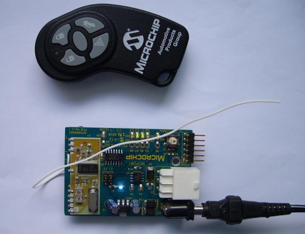
Anexa1: Poza dispozitivului PKE (Passive Keyless Entry)
Anexa2: Poza dispozitivului RKE (Remote Keyless Entry)
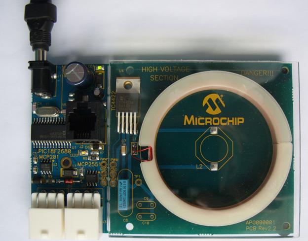
Anexa3: Poza modulului statiei baza
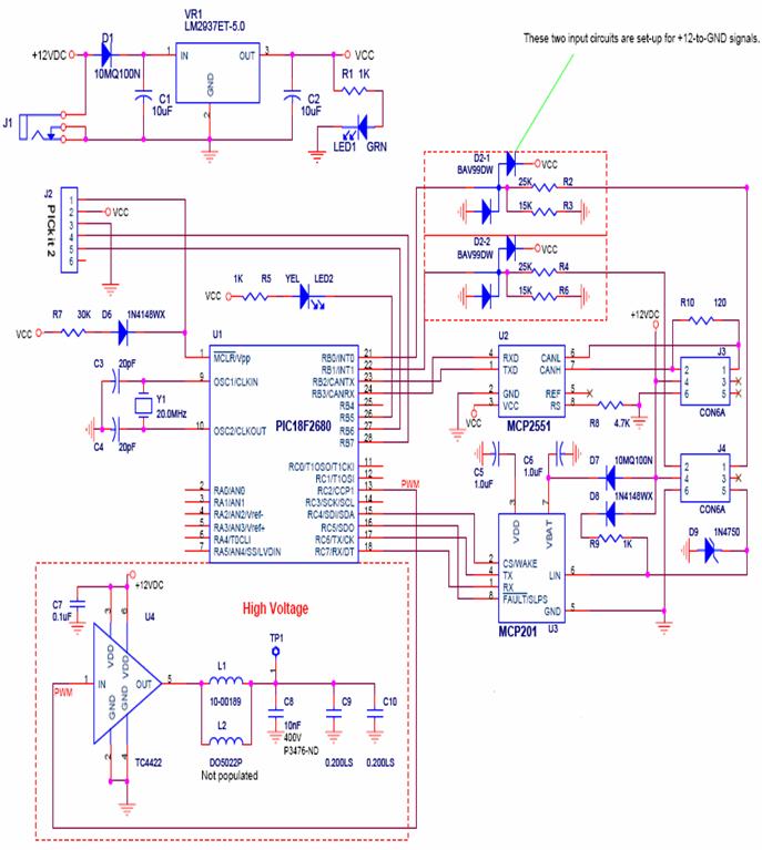
Anexa4: Schema circuitului statiei baza
Anexa5: Programul statiei baza
#include <p18f2680.inc>
ERRORLEVEL 0,-301,-302,-305, -226 ; Messages, Warnings and Errors Printed
; Ignore [301] => Processor Mismatch.
; Ignore [302] => Register in operand not in bank 0.
; Ignore Warning[226]: Destination address must be word aligned
__CONFIG _CONFIG1H, _OSC_HS_1H & _FCMENB_OFF_1H & _IESOB_OFF_1H
__CONFIG _CONFIG2L, _BOR_OFF_2L & _BORV_27_2L & _PWRT_ON_2L
__CONFIG _CONFIG2H, _WDT_OFF_2H & _WDTPS_128_2H
__CONFIG _CONFIG3H, _MCLRE_OFF_3H & _LPT1OSC_OFF_3H & _PBADEN_OFF_3H
__CONFIG _CONFIG4L, _XINST_OFF_4L & _LVP_OFF_4L & _STVREN_OFF_4L
; INCLUDE FILES
subtitle 'Data and Variable Definitions'
page
; USER DEFINED REGISTER
cblock 0x20
; COUNTER REGISTERS
CNT0,CNT1,CNT2,CNT3
CNT_HI
CNT_LW
;***** VARIABLE DEFINITIONS
w_temp
status_temp
pclath_temp
TEMP1
TEMP2
RXTX_REG
TEMP_COUNTER
COUNTER
CHAR
LSD
MSD
LCD_DATA_image
TEMP
pingcounter
resetbyte
MESSAGE_COUNTER ; Countes number of bytes to receive or transmit
ID_TEMP ; Register for ID byte
TEMP_TRANSFER ; Data transfer register
DATAPOINTER:10 ; address of data byte buffer
HdrID
ButtonImage
endc
TRANSMIT_OK EQU 0
;CNT_HI
bit_8s EQU 00000001B
bit_16s EQU 00000010B
bit_32s EQU 00000100B
bit_1m EQU 00001000B
bit_2m EQU 00010000B
bit_4m EQU 00100000B
bit_5m EQU 01000000B
bit_10m EQU 10000000B
;CNT_LW
bit_32ms EQU 00000001B
bit_64ms EQU 00000010B
bit_128ms EQU 00000100B
bit_256ms EQU 00001000B
bit_512ms EQU 00010000B
bit_1s EQU 00100000B
bit_2s EQU 01000000B
bit_4s EQU 10000000B
page
; ********* USER PORT DEFINITIONS *******
; ********* PORTA BIT DEFINITIONS *******
PA_CFG EQU B'11011000' ; PORTA : TRI-STATE VALUE
#define RS PORTA,0 ;LCD Command/Data Select
#define RW PORTA,1 ;LCD Read/Write Control
#define E PORTA,2 ;LCD E-strobe
#define LCD0 PORTA,3 ;LCD Data bit 0
#define LCD1 PORTA,4 ;LCD Data bit 1
#define BIAS PORTA,5 ; Receive Bias output control
LCD_CNTL_LAT EQU LATA
LCD_CNTL EQU PORTA
; ********* PORTB BIT DEFINITIONS *******
PB_CFG EQU B'11011011' ; PORTB : TRI-STATE VALUE
#define Button PORTB,0 ; Button SW1 Input
#define Ignition PORTB,1 ; Ignition ON Input
; #define CANTX PORTB,2 ; CAN Output
; #define CANRX PORTB,3 ; CAN Input
#define RFIN PORTB,4 ; RF INPUT
#define RedLED PORTB,5 ; VALID INDICATOR LED OUTPUT
; #define PORTB,6
; #define PORTB,7
; ********* PORTC BIT DEFINITIONS *******
PC_CFG EQU B'10101011' ; PORTC : TRI-STATE VALUE
#define LCD2 PORTC,0 ;LCD Data bit 2
#define LCD3 PORTC,1 ;LCD Data bit 3
#define PWM PORTC,2 ; LF PWM Output
; #define PORTC,3
#define CSwake PORTC,4 ; Chip Select / Wakeup output to LIN xcvr
#define FAULT_SLPS PORTC,5 ; Fault input / Slope Select output to LIN xcvr
#define CommTX PORTC,6 ; LIN Bus Transmit Output
#define CommRX PORTC,7 ; LIN Bus Receive Input
Dev_Freq EQU D'20000000' ; Device Frequency is 20 MHz
;LCD_INIT_DELAY EQU (HIGH ((( Dev_Freq / 4 ) * D'46' / D'10000' ) / 3 ) ) + 1
; LCD Module commands
DISP_ON EQU 0x0C ; Display on
DISP_ON_C EQU 0x0E ; Display on, Cursor on
DISP_ON_B EQU 0x0F ; Display on, Cursor on, Blink cursor
DISP_OFF EQU 0x08 ; Display off
CLR_DISP EQU 0x01 ; Clear the Display
ENTRY_INC EQU 0x06 ;
ENTRY_INC_S EQU 0x07 ;
ENTRY_DEC EQU 0x04 ;
ENTRY_DEC_S EQU 0x05 ;
DD_RAM_ADDR EQU 0x80 ; Least Significant 7-bit are for address
DD_RAM_UL EQU 0x80 ; Upper Left coner of the Display
BIT4LINE2 EQU 0x28
subtitle 'Initialization Code'
page
; PAGE 0:
ORG 00H
; FUNCTION : RESET ()
; DESCRIPTION : PROGRAM RESET ROUTINE
RESET_VECTOR
MOVLW PA_CFG ; UPDATE TRIS REGISTER FOR PORTA
MOVWF TRISA
MOVLW PB_CFG ; UPDATE TRIS REGISTER FOR PORTB
MOVWF TRISB
MOVLW PC_CFG ; UPDATE TRIS REGISTER FOR PORTC
MOVWF TRISC
CLRF PORTA ; RESET PORTA
MOVLW b'00110000'
movwf PORTB ; RESET PORTB
MOVLW b'11110000'
movwf PORTC ; RESET PORTC
; bsf RFIN
; bsf RedLED ;turn off red LED
CLRF STATUS ; Do initialization
CLRF INTCON
CLRF PIR1
CLRF PIE1 ; Disable all peripheral interrupts
MOVLW 0x07 ;
MOVWF ADCON1 ; Port A is Digital.
MOVLW B'00000111' ; SETUP TMR0 PRESCALER
MOVWF T0CON
BCF T1CON, TMR1ON ; Timer 1 is NOT incrementing
movlw .39 ; set PWM period to 8us
movwf PR2
movlw B'00000100' ; set TMR2 no postscaler,ON,1:1 prescaler
movwf T2CON
movlw (.39/2) ; set PWM duty cycle to 50%
movwf CCPR1L
clrf CCP1CON ; turn off PWM
; call StartUpRAMInit
; call Init_AUSART
; GOTO MAIN ; GOTO MAIN PROGRAM LOOP
subtitle ' '
page
subtitle 'Main Program Loop'
page
; FUNCTION : MAIN ()
; DESCRIPTION : MAIN PROGRAM ROUTINE
; movlw .20 ;delay 15mS for display to warm up
; movwf TEMP
;wait15ms
; call Delay1ms
; decfsz TEMP
; bra wait15ms
; bra POR_Display
;debuginit
; movlw .20 ;delay 15mS for display to warm up
; movwf TEMP
;wait15msa
; call Delay1ms
; decfsz TEMP
; bra wait15msa
; call INIT_DISPLAY
; bra POR_D0
;POR_Display
; bsf RCON,POR
; call DISPLAY_INIT
; bra debuginit
;POR_D0 call PaintMICROCHIP
; bsf RedLED ;turn off red LED
call SendWakeUp
BTFSC RFIN ; INPUT HIGH?
bra $-2
MAIN
movlw 0x03
movwf pingcounter
; BTFSS RFIN ; INPUT HIGH?
; GOTO CheckRFAnswerBack ; NO, JUMP OUT OF LOOP
RFButtonLoop
; BTFSC RFIN ; INPUT HIGH?
; bra RFButtonSeen ; NO, JUMP OUT OF LOOP
btfsc Button ; wait for button push
bra RFButtonLoop
WakeUpMessage
; call PaintPING
call SendWakeUp
call Delay50us
; btfsc RFIN
; bra $-2
CheckRFAnswerBack
RFBack2
MOVLW .50 ; 50 ms TIMER
MOVWF CNT1
RFBack0
MOVLW .200
MOVWF CNT0
RFBack1
; BTFSC RFIN ; INPUT HIGH?
; bra RFBackSeen ; NO, JUMP OUT OF LOOP
DECFSZ CNT0,1 ; YES, CONTINUE WITH TIMING LOOP
bra RFBack1 ; 5 us X CNT0
DECFSZ CNT1,1 ; DO 200 us LOOP CNT1 TIMES
bra RFBack0
bsf RedLED ; turn off red LED
; bra WakeUpMessage ; No answer back
; movlw 0x05
; movwf ID_TEMP
; movlw 0x03
; movwf DATAPOINTER
; call SendLINcommand
; decfsz pingcounter
; bra WakeUpMessage
bra MAIN
;RFBackSeen
;Validate4mSheaderHIGH
movlw .10 ;.40 anything longer than 1mS is OK
movwf TEMP2
;V4mSH1 movlw .48 ; 1 cycle
movwf TEMP1 ; 1 cycle
; time=((X*5)+7)*(1/(Fosc/4))
;V4mSH0 btfss RFIN ; 2 cycles
bra RecvUHF_FAIL ; 2 cycles
decfsz TEMP1, f ; 1 cycle
bra V4mSH0 ; 2 cycles
decfsz TEMP2,f
bra V4mSH1
btfsc RFIN ; 2 cycles, wait for falling edge
bra $-2
;Validate500uSheaderLOW
movlw .8
movwf TEMP2
;V500uSL1 movlw .48 ; 1 cycle
movwf TEMP1 ; 1 cycle
; time=((X*5)+7)*(1/(Fosc/4))
;V500uSL0 btfsc RFIN ; 2 cycles
bra RecvUHF_FAIL ; 2 cycles
decfsz TEMP1, f ; 1 cycle
bra V500uSL0 ; 2 cycles
decfsz TEMP2,f
bra V500uSL1
btfss RFIN ; 2 cycles, wait for rising edge
bra $-2
;Validate2mSheaderHIGH
movlw .30 ;.40
movwf TEMP2
;V2mSH1 movlw .48 ; 1 cycle
movwf TEMP1 ; 1 cycle
; ; time=((X*5)+7)*(1/(Fosc/4))
;V2mSH0 btfss RFIN ; 2 cycles
bra RecvUHF_FAIL ; 2 cycles
decfsz TEMP1, f ; 1 cycle
bra V2mSH0 ; 2 cycles
decfsz TEMP2,f
bra V2mSH1
btfsc RFIN ; 2 cycles, wait for falling edge
bra $-2
;Validate2mSheaderLOW
movlw .30 ;.40
movwf TEMP2
;V2mSL1 movlw .48 ; 1 cycle
movwf TEMP1 ; 1 cycle
; time=((X*5)+7)*(1/(Fosc/4))
;V2mSL0 btfsc RFIN ; 2 cycles
bra RecvUHF_FAIL ; 2 cycles
decfsz TEMP1, f ; 1 cycle
bra V2mSL0 ; 2 cycles
decfsz TEMP2,f
bra V2mSL1
btfss RFIN ; 2 cycles, wait for rising edge
bra $-2
; movlw .4 ; number of bits to receive
; movwf COUNTER ; load number of bits into counter register
; call ReceiveNext
; movf RXTX_REG,w
; movwf HdrID
;get button data byte
; movlw .8 ; number of bits to receive
; movwf COUNTER ; load number of bits into counter register
; call ReceiveNext
; movf RXTX_REG,w
; movwf ButtonImage
; swapf HdrID,w
; andlw 0x0F
; xorlw 0x05
; btfsc STATUS,Z
; bra GoodUHFBack
; call PaintBADResp
; btfss STATUS,Z
; bsf RedLED ; turn off red LED
; nop
; movlw .200
; movwf CNT1
;BUHFB0 call Delay4ms
; decfsz CNT1
; bra BUHFB0
; goto MAIN
;GoodUHFBack
; bcf RedLED ; turn on red LED
; movlw 0x05
; movwf ID_TEMP
; movlw 0x01
; movwf DATAPOINTER
; call SendLINcommand
; call PaintGOODResp
; movlw .50
; movwf CNT1
;GUHFB0 call Delay4ms
; decfsz CNT1
; bra GUHFB0
; goto MAIN
;RecvUHF_FAIL
; bsf RedLED ;turn off red LED
; call PaintBADUHF
; bcf mark
; bra RFBack1
;RFButtonSeen
;AuxValidate4mSheaderHIGH
movlw .10 ;.40 anything longer than 1mS is OK
movwf TEMP2
;AuxV4mSH1 movlw .48 ; 1 cycle
movwf TEMP1 ; 1 cycle
; ; time=((X*5)+7)*(1/(Fosc/4))
;AuxV4mSH0 btfss RFIN ; 2 cycles
bra RecvUHF_buttonFAIL ; 2 cycles
decfsz TEMP1, f ; 1 cycle
bra AuxV4mSH0 ; 2 cycles
decfsz TEMP2,f
bra AuxV4mSH1
btfsc RFIN ; 2 cycles, wait for falling edge
bra $-2
;AuxValidate500uSheaderLOW
movlw .8
movwf TEMP2
;AuxV500uSL1 movlw .48 ; 1 cycle
movwf TEMP1 ; 1 cycle
; ; time=((X*5)+7)*(1/(Fosc/4))
;AuxV500uSL0 btfsc RFIN ; 2 cycles
bra RecvUHF_buttonFAIL ; 2 cycles
decfsz TEMP1, f ; 1 cycle
bra AuxV500uSL0 ; 2 cycles
decfsz TEMP2,f
bra AuxV500uSL1
; MOVLW .200
; MOVWF CNT0
;RF1
; BTFSC RFIN ; INPUT HIGH?
; bra AuxValidate2mSheaderHIGH ; NO, JUMP OUT OF LOOP
; DECFSZ CNT0,1 ; YES, CONTINUE WITH TIMING LOOP
; bra RF1 ; 5 us X CNT0
; bra RecvUHF_buttonFAIL ; 2 cycles
btfss RFIN ; 2 cycles, wait for rising edge
bra $-2
;AuxValidate2mSheaderHIGH
movlw .30 ;.40
movwf TEMP2
;AuxV2mSH1 movlw .48 ; 1 cycle
movwf TEMP1 ; 1 cycle
; time=((X*5)+7)*(1/(Fosc/4))
;AuxV2mSH0 btfss RFIN ; 2 cycles
bra RecvUHF_buttonFAIL ; 2 cycles
decfsz TEMP1, f ; 1 cycle
bra AuxV2mSH0 ; 2 cycles
decfsz TEMP2,f
bra AuxV2mSH1
btfsc RFIN ; 2 cycles, wait for falling edge
bra $-2
;AuxValidate2mSheaderLOW
movlw .30 ;.40
movwf TEMP2
;AuxV2mSL1 movlw .48 ; 1 cycle
movwf TEMP1 ; 1 cycle
; time=((X*5)+7)*(1/(Fosc/4))
;AuxV2mSL0 btfsc RFIN ; 2 cycles
bra RecvUHF_buttonFAIL ; 2 cycles
decfsz TEMP1, f ; 1 cycle
bra AuxV2mSL0 ; 2 cycles
decfsz TEMP2,f
bra AuxV2mSL1
btfss RFIN ; 2 cycles, wait for rising edge
bra $-2
; movlw .4 ; number of bits to receive
; movwf COUNTER ; load number of bits into counter register
; call ReceiveNext
; movf RXTX_REG,w
; movwf HdrID
;get button data byte
; movlw .8 ; number of bits to receive
; movwf COUNTER ; load number of bits into counter register
; call ReceiveNext
; movf RXTX_REG,w
; movwf ButtonImage
; swapf HdrID,w
; andlw 0x0F
; xorlw 0x05
; btfsc STATUS,Z
; bra GoodUHFframe
; goto Wait200msLoop
;GoodUHFframe
; bcf RedLED ; turn on red LED
; movf ButtonImage,w
; xorlw 0x1B
; btfsc STATUS,Z
; goto SendUnLockCmd
; movf ButtonImage,w
; xorlw 0x17
; btfsc STATUS,Z
; goto SendLockCmd
; bsf RedLED ;turn off red LED
; bra MAIN
;SendUnLockCmd
; movlw 0x05
; movwf ID_TEMP
; movlw 0x02
; movwf DATAPOINTER
; call SendLINcommand
; goto Wait200msLoop
;SendLockCmd
; movlw 0x05
; movwf ID_TEMP
; movlw 0x01
; movwf DATAPOINTER
; call SendLINcommand
; goto Wait200msLoop
Wait200msLoop
movlw .50
movwf CNT1
GUHFf0 call Delay4ms
decfsz CNT1
bra GUHFf0
goto MAIN
;RecvUHF_buttonFAIL
; bsf RedLED ;turn off red LED
; bra MAIN
; ** ** ** ** ** ** ** ** ** ** *
; * Delay routines *
; ** ** ** ** ** ** ** ** ** ** *
Delay250us movlw .5
movwf TEMP2
BaseDelay call Delay50us
decfsz TEMP2,f
bra BaseDelay
return
Delay500us movlw .10
movwf TEMP2
bra BaseDelay
Delay2ms movlw .40
movwf TEMP2
bra BaseDelay
Delay4ms movlw .80
movwf TEMP2
bra BaseDelay
Delay1ms movlw .20
movwf TEMP2
bra BaseDelay
Delay350us movlw .7
movwf TEMP2
bra BaseDelay
Delay400us movlw .8
movwf TEMP2
bra BaseDelay
; time=((X*3)+6)*(1/(Fosc/4))
Delay50us movlw .81 ; 1 cycle + 2 cycles for CALL
movwf TEMP1 ; 1 cycle
decfsz TEMP1, f ; 1 cycle
bra $-2 ; 2 cycles
return ; 2 cycles + 1 cyclec for DECFSZ
; ** ** ** ** ** ** ** ** ** ** *
; * SendWakeUp frame routine *
; ** ** ** ** ** ** ** ** ** ** *
SendWakeUp
movlw 0x0C ; PWM on
movwf CCP1CON ; turn on PWM
call Delay4ms ; generate Delay for 4ms
clrf CCP1CON ; turn off PWM
call Delay500us ; generate Delay for 500us
movlw 0x0C ; PWM on
movwf CCP1CON ; turn on PWM
call Delay2ms ; generate Delay for 2ms
clrf CCP1CON ; turn off PWM
call Delay2ms ; generate Delay for 2ms
movlw 0x55
movwf RXTX_REG ; Send 0
movlw .4 ; four bits
movwf TEMP_COUNTER
call TransmitNext
return
; ** ** ** ** ** ** ** ** ** ** *
; * Low Frequency Transmit routine *
; ** ** ** ** ** ** ** ** ** ** *
Transmit8 movlw .8
movwf TEMP_COUNTER ; initialize count register
TransmitNext
rrcf RXTX_REG, f ; rotate receive register
btfsc STATUS, C ; test bit to be transmited
bra SendOne ; send high value
SendZero
movlw 0x0C ; PWM on
movwf CCP1CON ; turn off PWM
call Delay500us ; delay for 500us
clrf CCP1CON ; turn off PWM
call Delay250us ; delay for 250us
bra SendNextBit ; send next bit
SendOne
movlw 0x0C ; PWM on
movwf CCP1CON ; turn off PWM
call Delay250us ; delay for 250us
clrf CCP1CON ; turn off PWM
call Delay500us ; delay for 500us
bra SendNextBit ; send next bit
SendNextBit decfsz TEMP_COUNTER, f ; decrement counter register
bra TransmitNext ; transmit next bit
retlw TRANSMIT_OK ; return to main routine
; ** ** ** ** ** ** ** ** ** ** *
; * Receive Routine *
; ** ** ** ** ** ** ** ** ** ** *
Receive8
clrf RXTX_REG ; clear receive register
movlw .8 ; number of bits to receive
movwf COUNTER ; load number of bits into counter register
ReceiveNext
btfss RFIN ; test for rising edge
bra ReceiveNext
call Delay350us ; wait until middle of bit
btfsc RFIN ; is RFIN zero or a one?
bcf STATUS,C ; bit is a one => set carry bit
btfss RFIN ; is RFIN one or a zero?
bsf STATUS,C ; RFIN is zero => clear carry bit
rrcf RXTX_REG, f ; rotate value into receive register
btfsc RFIN ; wait for bit to go low
bra $-2
decfsz COUNTER, f ; decrement receive count register by one
bra ReceiveNext ; receive next bit
ReceiveLastBit
btfsc RFIN ; wait until end of last bit
goto ReceiveLastBit
call Delay400us ; wait until end of last bit
retlw 0x00 ; return
; #include <AUSARTmstr.asm>
; END OF FILE :
END
Anexa6: Poza modulului emitator-transponder

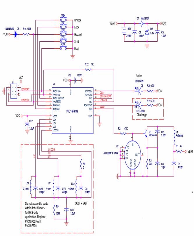
Anexa5. Schema circuitului emitator-transponder
Anexa8:Poza modulului receptor/decoder
Anexa9: Schema circuitului receptor/decoder
| Contact |- ia legatura cu noi -| | |
| Adauga document |- pune-ti documente online -| | |
| Termeni & conditii de utilizare |- politica de cookies si de confidentialitate -| | |
| Copyright © |- 2025 - Toate drepturile rezervate -| |
|
|
||||||||||
|
||||||||||
Referate pe aceeasi tema
| ||||||||||
|
| ||||||||||
|
||||||||||
|
|
||||||||||